DL-CC1310-B433, 433MHz Wireless Transparent, SoC Transceiver Module, TI CC1310 Chip
-
 DL-CC1310-B433
 - 433Mhz
- CC1310
- +14dBm
- 1.8~3.8V
- -122dBm
- 800m
- 18*16*2mm
Brief Introduction
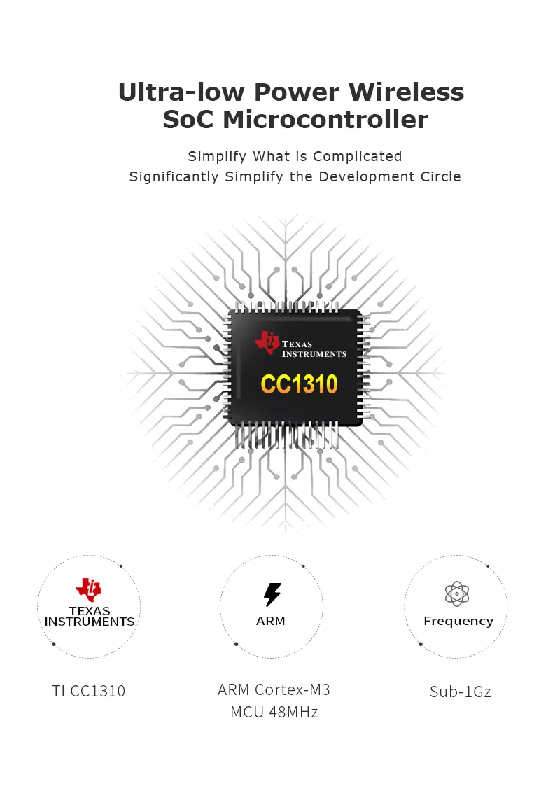
DL-CC1310-B Wireless Module is a SoC embedded Serial Port RF Transceiver Module (UART Module) with AT command, which was developed by DREAMLNK based on TI' CC1310 (built-in dual-core ARM) Radio Frequency chip. It combines an integrated RF Controller (Cortex®-MO) and a powerful Arm® Cortex®-M3 Processor, the Clock Speed of the MCU can reach up to 48MHz.
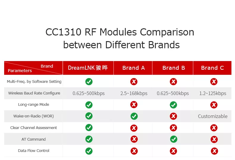
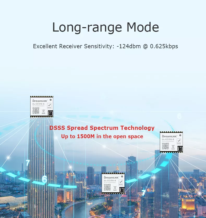
This DL-CC1310-B Wireless Module supports Narrow-band Communication, Direct Sequence Spread Spectrum (DSSS), Long-range Transmission and High-efficiency Communication. It has built-in fully functional AT Commands that support any Serial Baud Rate setting from 1920bps to 256000bps, which can greatly improve the communication efficiency with up to -124dBm receiver sensitivity.
The embedded software makes this Wireless Module support not only Transparent Transmission Mode, Accurate Signal Strength Indication, automatic CCA (Clear Channel Assessment), but also High-speed Data Stream & Packet Segmentation Transmission, which can effectively reduce the probability of signal collision.
Hardware Features:
● Original CC1310 Chip from TI;
● SOC integrated RF module with metal shield
● Industrial grade components: 433/868/915MHz
● Wide supply voltage range: 1.8V to 3.8V;
● Ultra-low sleep current < 1uA;
● High efficiency receiving performance (RX current @ 5.5mA);
● High Transmission Efficiency:
TX (+10dBm): 17mA;
TX (+14dbm): 27mA;
● Excellent Receiver Sensitivity:
Long Range Mode: -124dbm at 0.625kbps;
Universal Mode: -110dbm at 50kbps;
● Accurate Signal Strength Indication and Clear Channel Assessment (CCA).
● Compact size for SMD mounting (Dimensions = 18x16.5mm)
Software Features:
● Easily configure with defaulted AT command, for a simple development;
● Transparent Transmission Mode supported;
● Data flow control & high-speed data stream transmission supported;
● 1920-256000bps serial baud rate is supported;
● 0.6kbps-500kbps wireless baud rate is supported;
● Wake-on-Radio (eWOR) function supported, which can be greatly increases the battery standby time;
● Packet Segmentation Supported
● Preset CCA (Clear Channel Assessment) function, which can effectively reduce the collision probability of co-frequency interference;
● Strong Anti-jamming: supports anytime RSSI acquisition and CCA (Clear Channel Assessment);
● Supports manual fast frequency hopping to avoid co-frequency interference;
● Point-to-Point, Broadcasting and Monitoring transmission can be achieved.
Technical Parameter
Recommended Configuration


|
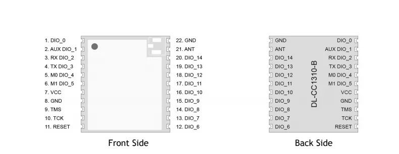
Pin Name |
I/O Type |
Pin Description |
|
VCC |
PWR |
To maximize the chip function, ≥2.5V stable voltage is recommended |
|
GND |
PWR |
Reference Ground |
|
ANT |
Analog I/O |
RF signal input/output port, π-matching network must be reserved; Adopt 50Ω impedance matching for RF routing, route the ground and add via holes around it |
|
DIO1(AUX) |
Out |
Indicate the working status of the module:
Start-up initialization or wake-up mode initialization: 0: Initialization completed; serial port transmission can be carried out 1: Serial port transmission is not allowed until initialization is completed
AT Command: 0: Idle 1: TX buffer is full and needs to wait for low level before transmission
Transparent Transmission Mode & Wake-on-Radio (WOR) Mode: 0: Idle 1: The module receives the data and outputs the data through the serial port after the set delay
When Transmitting Data to the Module: 0: The buffer is empty (Transmitting completed) / the buffer is not full 1: Buffer is not empty / buffer full, (Two settings can be configured by "AT+ AUXM” Command) |
|
DIO2(UART-RX) |
In |
TTL serial port input, connected to external TXD output pin |
|
DIO3(UART-TX) |
Out |
TTL serial port output, connected to external RXD input pin |
|
DIO4(M0) |
In |
Switching between AT Command and Transparent Transmission Mode, defaulted high level 0: Transparent Transmission Mode 1: AT Command Mode |
|
DIO5(M1) |
In |
Control Module Sleep, defaulted high level 0: Sleep (or wake-on-radio) 1: Wake up |
|
DIO6-DIO14 |
Out / In |
Common I/O port, no function at present, can be customized to realize the following functions: 1. ADC detection 2. Key value fast transmit 3. RF status indication 4. PA control If not used, it must be N/C (No Connection) |


