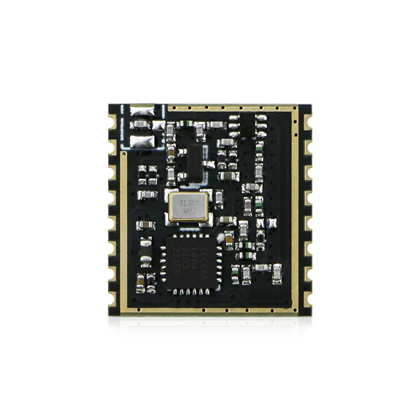
DL-LLCC68-S-433, 433MHz Wireless LoRa Module High Sensitivity LLCC68
-
 DL-LLCC68-S-433
 - 433Mhz
- LLCC68
+22dBm- 0.3~3.6V
-129dBm- 3000m
- 17.1*16.1*2mm
433MHz/868MHz/915MHz Wireless LoRa Transceiver Module with LLCC86 Chip
DL-LLCC68-S is a wireless module designed based on Semtech's radio frequency chip LLCC68. It mainly adopts a new generation of LoRa™ modulation technology for ultra-long-distance spread spectrum communication. This LoRa module is compact in size, and has the characteristics of ultra-low receiving power consumption, strong anti-interference ability, and longer transmission distance than traditional modulation methods. It can be widely used in various wireless communication fields of the Internet of Things.
DL-LLCC68-S RF module has high receiving sensitivity of -129dBm@LoRa, ultra-low receiving current and dormant current, the transmit power can be configured through software, and the maximum power can reach +22dBm. Compared with traditional modulation technology, LoRa™ modulation technology has obvious advantages in anti-blocking and selection, which solves the problem of distance, anti-interference and power consumption that traditional design schemes cannot take into account at the same time.
Applications
● ISM band data communication
● Intelligent buildings
● Smart home Security
● AMR (Automatic Message Recording)
● Wireless remote control
● Building automation
● Wireless sensor network
● Energy control and management
● RKE (Remote Keyless Entry)
● Thermal energy collection, meter measurement

Features & Brief Introduction
● Support (G)FSK, LoRa™ and other modulation methods;
● The chip supports a frequency range of 150~960MHz;
● Recommended frequency: 433/470MHz => 433M LoRa module; 868/915MHz => 868/915M LoRa module;
● The working voltage is 3.3V, the maximum output transmitting power is +22dBm, and the maximum working current is 130mA;
● It has low power consumption characteristics in the receiving state, the minimum receiving current is 4.5mA, and the standby current is 0.6mA;
● High receiving sensitivity: -129dBm@LoRa;
● Automatic Channel Activity Detection (CAD) with ultra-fast AFC
● Support spreading factor: SF5/SF6/SF7/SF8/SF9/SF10/SF11;
● Supported bandwidth: 125kHz, 250kHz, 500kHz
BW = 125kHz @ SF5-SF9
BW = 250kHz @ SF5-SF10
BW = 500kHz @ SF5-SF11


|
No |
Definitions |
Description |
|
|
1 |
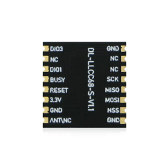
ANT/NC |
AI/AO |
Antenna interface, 50Ω impedance, ground and via hole |
|
2 |
GND |
PWR |
Reliable grounding |
|
3 |
3.3V |
PWR |
To maximize the chip function, 3.3V stable voltage is recommended |
|
4 |
RESET |
I |
Reset to initialize the chip, for an increased stability. High level as defaulted, while low level to reset the chip |
|
5 |
BUSY |
O |
The internal status indicator pin of the chip, which needs to be connected to the GPIO of the master MCU |
|
6 |
DIO1 |
IO |
Digital I/O 1 port, Configurable via software |
|
7 |
NC |
|
No connection |
|
8 |
DIO3 |
IO |
Digital I/O 3 port, Configurable via software |
|
9 |
GND |
PWR |
Reliable grounding |
|
10 |
NC |
No connection |
|
|
11 |
NC |
|
No connection |
|
12 |
SCK |
I |
SPI Serial Clock Input |
|
13 |
MISO |
O |
SPI Master Input Slave Output |
|
14 |
MOSI |
I |
SPI Master Output Slave Input |
|
15 |
NSS |
I |
SPI Chip Select Input |
|
16 |
GND |
PWR |
Reliable grounding |


