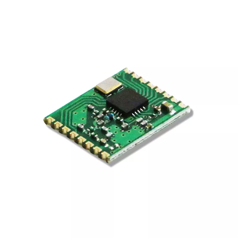
DL-RTS4438B,433MHz FSK Transceiver module with Si4438 chip, low-power, long-distance
-
 DL-RTS4438B
 - 433Mhz
- Si4438
-20~20dBm- -0.3~3V
-124dBm- 1800m
- 15*12.5*2mm
High-performance FSK Transceiver Module with Si4438 chip
Module introduction
DL-RTS4438B was designed base on Silicon Labs' Si4438 wireless transceiver chip. It is a compact,low-power, long distance wireless transceiver module. The chip launched by Silicon Labs is mainly set to 433MHz, 470MHz, 510MHz frequency bands of the national networks. The sensitivity can reach -124dbm, the maximum transmission rate can reach 500Kbps, and the output power can range from -20dbm to + 20dbm through the register configuration. The module integrates all RF-related functions. Users do not need to have a deep understanding of RF circuit design; they can use this module to easily develop wireless products with stable performance and high reliability,shortening the product development cycle.The module adopts single-chip architecture, and the periphery adopts high-precision crystal, high-Q Murata inductor, small volume but high-capacity filter capacitor. All SMD components are used, and the interface is encapsulated with standard pitch stamps, which is conducive to the development of compact systems and the application of mass placement.
Features
● 1800 meters transmission distance (1200bps);
● Working frequency 433.92M
● Working voltage: 1.8V-3.6V
● The receiving working current is only 14mA, which is lower than the industry level
● The interface uses an efficient 4-line SPI interface
● Independent 64-byte RX FIFO and TX FIFO
● Support WOR wireless signal wake-up function for portable devices
Applications
● Wireless sensor;
● Home automation;
● Automated data collection;
● Industrial remote control, telemetry;
● Data monitoring and transmission;
● Home Appliance Control;
● Security, alarm control;
Technical Parameter
DC characteristics
RF characteristics (Unless otherwise stated, the temperature is 25 ℃, and VCC is 3.3V)

| Pin | Name | Description | Remark |
| 1 | VDD | Power supply 3.3V | RF VDD |
| 2 | TXRAMP | Output of external PA, not used | |
| 3 | GPIO_0 | GPIO0 pin directly connected to the chip | |
| 4 | GPIO_1 | GPIO1 pin directly connected to the chip |
Configuration register |
| 5 | NIRQ |
Interrupt input pin, output low level when interrupt is generated |
|
| 6 | SCLK | SCLK input. Provide four-line serial data clock function | |
| 7 | MISO | 0~VDD Digital output | |
| 8 | MOSI | 0~VDD Digital input | |
| 9 | NSEL | Input pin for serial interface select | |
| 10 | GPIO_2 | GPIO2 pin directly connected to the chip | |
| 11 | GPIO_3 | GPIO3 pin directly connected to the chip | |
| 12 | SDN | Turn off input pin, SDN = 0 or 1; Refer to IC specification | |
| 15 | ANT | Antenna interface, 50Ω standard impedanc | |
| 14、16 | GND | Grounding, common ground with the system | 13 pins NC |


