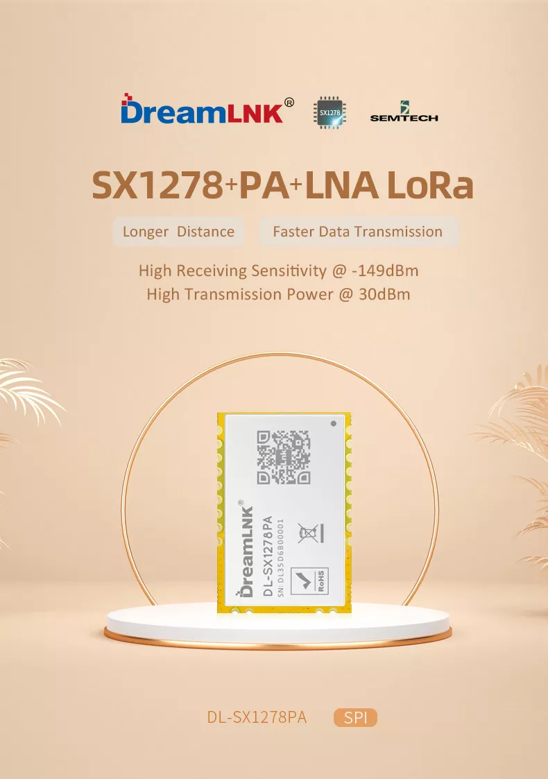
DL-SX1278PA, 433MHz SX1278 High Power Wireless LoRa Module with PA & LNA (433/470Mhz)
-
 DL-SX1278PA
 - 433Mhz
- SX1278
+30dBm- 3.3~5.5V
-149dBm- 6000m
- 37*25*4mm
433MHz Wireless LoRa Transceiver Module with SX1278 Chip
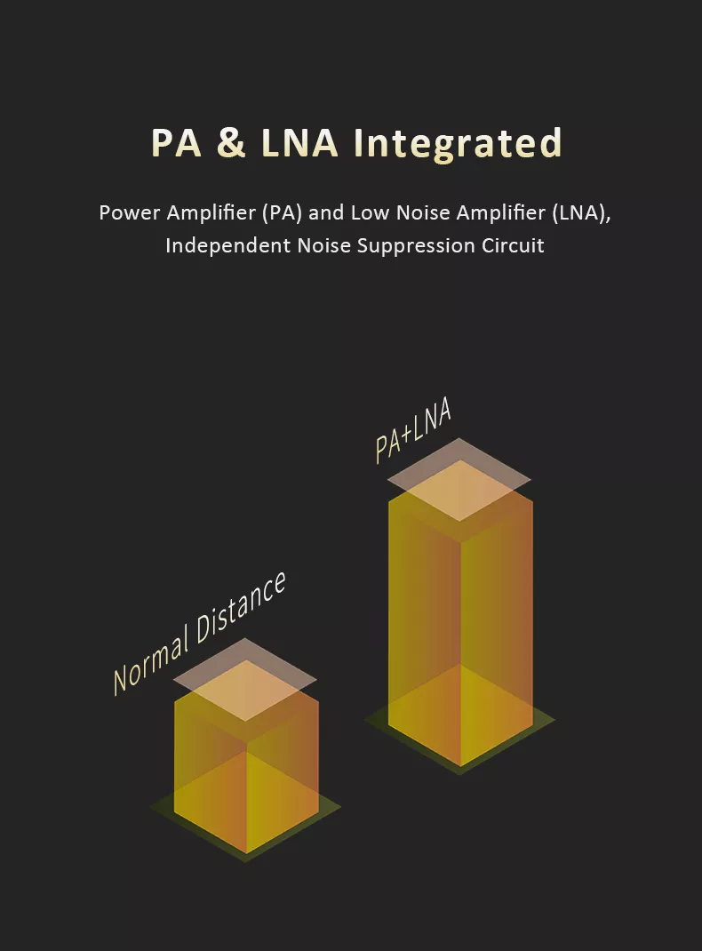
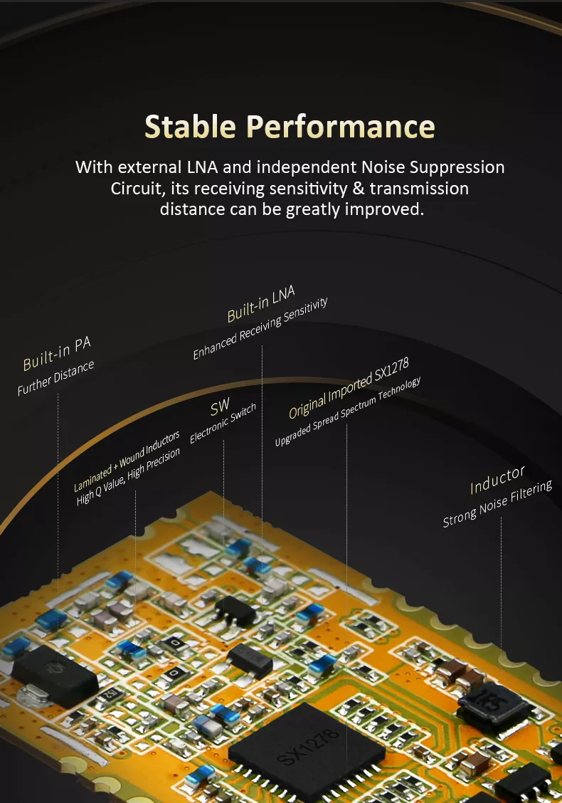
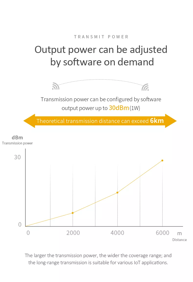
DL-SX1278PA is a high power 433Mhz LoRa Transceiver Module, which was developed by DREAMLNK based on Semtech's RF chip SX1278. For long-range transmission and better coverage concern, a power amplifier (PA) and a low noise amplifier (LNA) are integrated in this LoRa module, which improves its output power (up to 1W) by more than three times of the original SX1278 chip. Meanwhile, its receiving sensitivity has been greatly improved, with its sufficient link budget and advanced LoRa™ spread spectrum technology, this LoRa Module can achieve a longer transmitting distance.
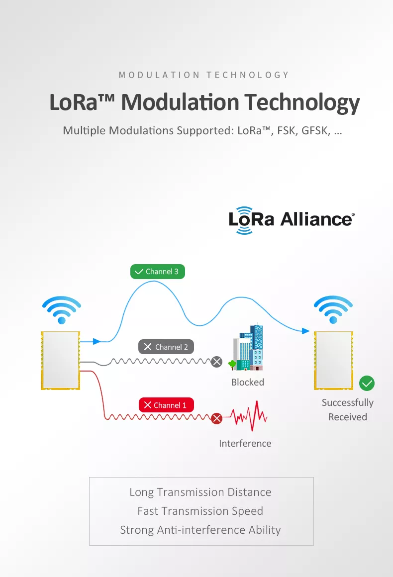
The output power can be configured by software, and the maximum output power of the module can be up to 30dBm. Compare with traditional modulation (FSK/GFSK) technology, this LoRa™ Modulation technology has obvious advantages in receiving current, receiving sensitivity, transmitting power, receiving rate range and anti-interference ability. It solves the problems of Transmission Distance, Anti-interference, Signal Blind Angle and Power Consumption that the traditional modulation cannot take into account at the same time.
With the help of LoRa™ Modulation technology, this DL-SX1278PA RF Transceiver Module can achieve Max. -149dBm@LoRa receiving sensitivity. It has more concentrated power density and better stability, with also many other advantages, such as low power consumption, long transmission distance, strong anti-interference performance, high confidentiality and strong concealment.
Features
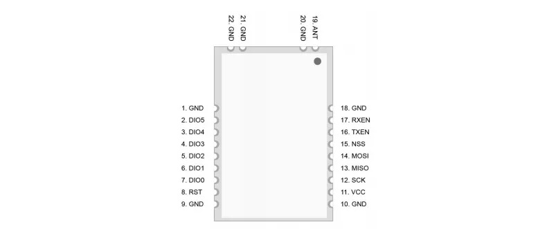
|
No |
Definitions |
Type |
Description |
|
1 |
GND |
PWR |
Reliable grounding |
|
2 |
DIO5 |
I/O |
General Digital I/O port, Configurable via software |
|
3 |
DIO4 |
I/O |
General Digital I/O port, Configurable via software |
|
4 |
DIO3 |
I/O |
General Digital I/O port, Configurable via software |
|
5 |
DIO2 |
I/O |
General Digital I/O port, Configurable via software |
|
6 |
DIO1 |
I/O |
General Digital I/O port, Configurable via software |
|
7 |
DIO0 |
I/O |
General Digital I/O port, Configurable via software |
|
8 |
RST |
I |
Chip reset trigger input pin, active low level |
|
9 |
GND |
PWR |
Reliable grounding |
|
10 |
GND |
PWR |
Reliable grounding |
|
11 |
VCC |
PWR |
Power supply, range 4.75~5.5V (it is recommended to add ceramic filter capacitor externally) |
|
12 |
SCK |
I |
SPI Serial Clock Input |
|
13 |
MISO |
O |
SPI Master Input Slave Output |
|
14 |
MOSI |
I |
SPI Master Output Slave Input |
|
15 |
NSS |
I |
SPI Chip Select Input, used to start/end an SPI communication |
|
16 |
TXEN |
I |
RF switch pin control; when transmission, TXEN is high level, and RXEN is low level |
|
17 |
RXEN |
I |
RF switch pin control; when receiving, RXEN is high level, and TXEN is low level |
|
18 |
GND |
PWR |
Reliable grounding |
|
19 |
ANT |
A IO |
Analog antenna interface, 50Ω impedance |
|
20/21/22 |
GND |
PWR |
Reliable grounding |


